Getting PCB Curing Right with Gallium Iodide
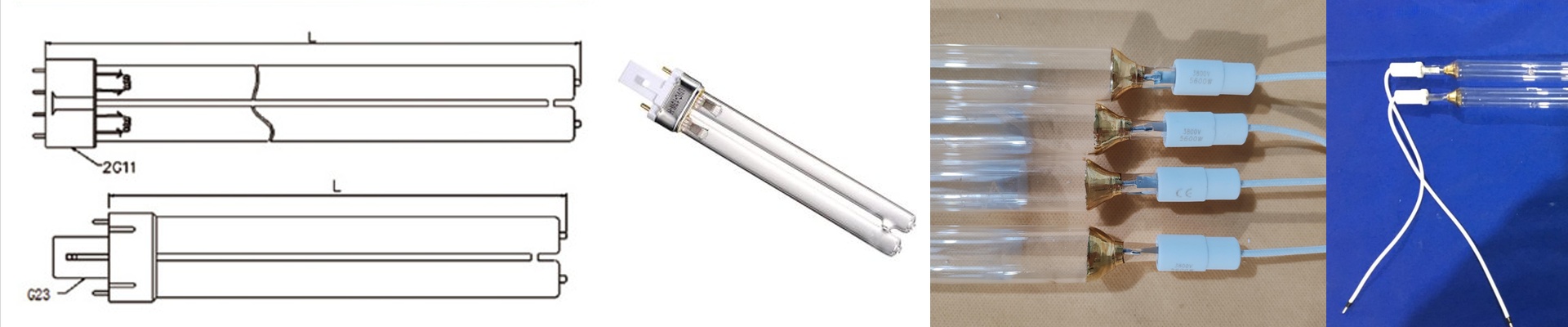
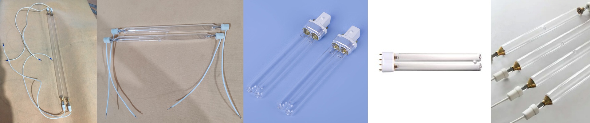
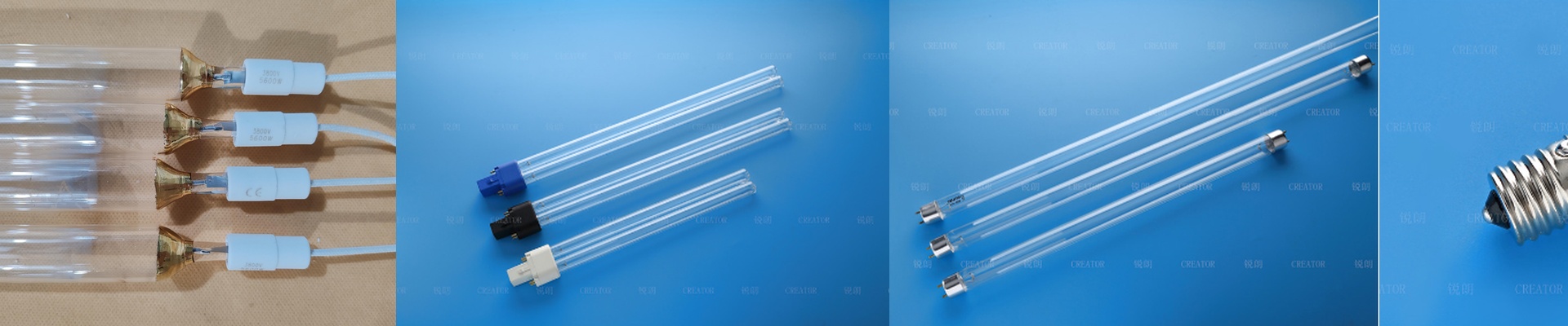
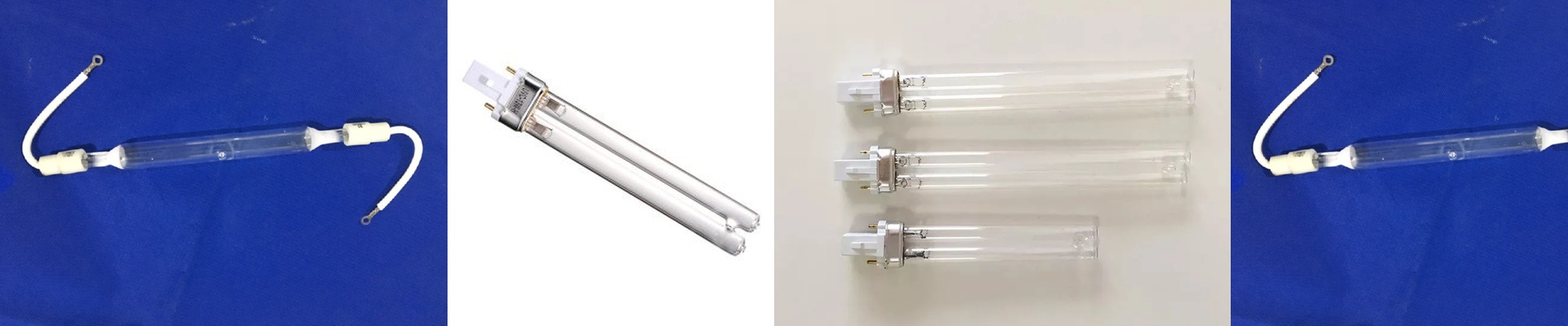
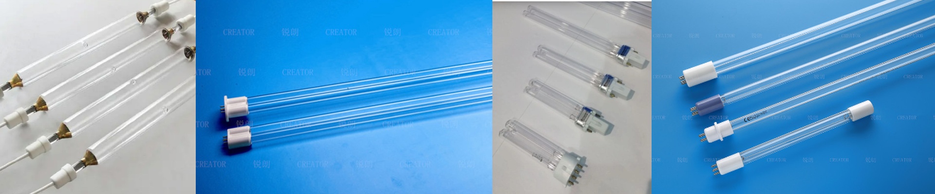
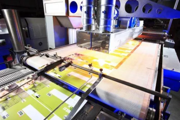
We build Gallium Iodide (GaI) lamps for the people who have to deal with the nightmare of tight tolerances in PCB factories. Standard mercury lamps are fine for some things, but they aren’t precise. GaI technology is different. It shifts the light spectrum to hit exactly what the photoresist needs. That’s why people were hovering around our modules at the 2026 print show—we’ve finally figured out how to stop that annoying depth-of-cure problem in HDI boards. The science part (simplified) Here is how it works: these lamps pump out high-intensity UV radiation between 250nm and 350nm. We tune them to hit the peak absorption frequency of your resist. The result? Your boards cure faster, but the substrate doesn’t overheat. Because the spectral band is so narrow, you don’t get that “stray light” that usually blurs the edges of your fine circuit traces. Everything just stays sharp. The hardware side of things We use high-purity quartz envelopes so the UV light doesn’t get blocked or weakened. Then, we wire them into custom arrays so the light hits every inch of the PCB panel evenly. But a word of warning: you can’t just plug these into any old ballast. You need precise current control, or you’ll burn out the electrodes way too fast. And then there’s the heat. GaI lamps run hot. Like, really hot. If your conveyor cooling isn’t up to the task, your substrates will warp. We usually suggest adding integrated air-cooling manifolds to keep things stable. What this means for your shop floor For the engineers, this is a relief. It’s a drop-in replacement for those aging mercury systems. You get cleaner lines and your cycles get shorter. We spent a lot of time on the footprint, too. We wanted to make sure these fit into your existing curing tunnels so you don’t have to tear down and rebuild your whole machine. If you’re pushing for 2 micron trace widths, you’re going to need this kind of spectral purity. It’s the only way to make sure those lower layers actually cure properly.